


印刷电子实验室 >研发中心 >研发中心
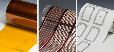
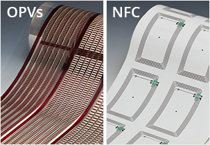
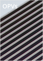
专业用于印刷电子柔性材料行业包括OPV太阳能电池,OLED,照明,智能ID卡或者其他柔性材料产品的工艺和设备开发。 我们超过55年的专业设计制造卷对卷的加工设备的技术和专业技能使我们能够成为这个快速增长行业的主导者。我们的宗旨是专注系统整合,用先进的涂布/印刷科技,精密套准系统和交钥匙设备为印刷电子行业的客户提供全面支持。
SPEL for Printed Intelligence
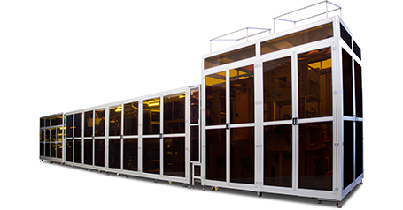
SungAn Printed Electronics Laboratory specializes in developing process technology for various printed electronic applications such as organic photovoltaic (OPV), organic light emitting diode (OLED) lighting and others. During the last decade, SPEL has been focused on developing the various fabrication processes, which is composed with printing, coating and drying technology including machine and control system. The turn key system technology, with roll to roll based process and unique know-how of printing, coating and drying offers reliable mass production to whomever wants to start the flexible electronic business. 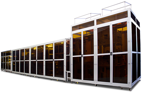
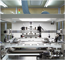
RCC Series
Applications
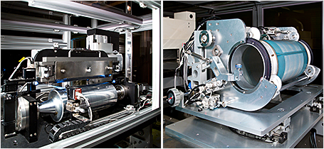
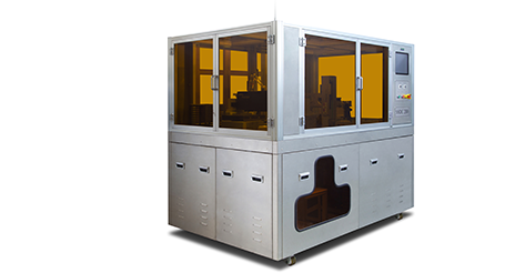
RSC-P Series
Applications
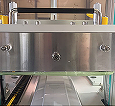
SSDC Series
Applications
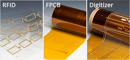
Core technology of printed electronics
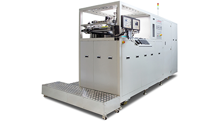
R2R based direct metal etching system
Advantage of direct metal etching paste Conventional wet etching process 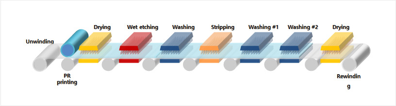
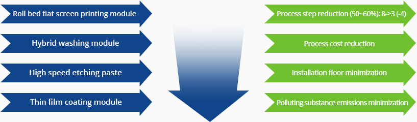
R2R hybrid etching process (with etching paste) 
Ultra high quality barrier film production system
Advantage of SAM’s ultra high barrier technology
Conventional barrier film tech 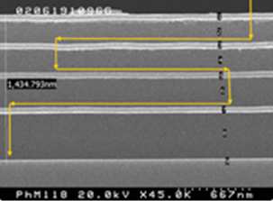
Increase moisture/ oxygen diffusion path length 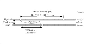
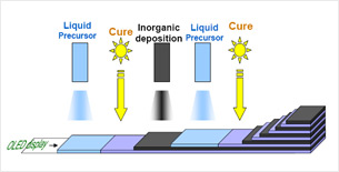

SAM’s barrier film tech 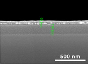
Reduce defect / pinhole of layer 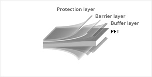
|
