


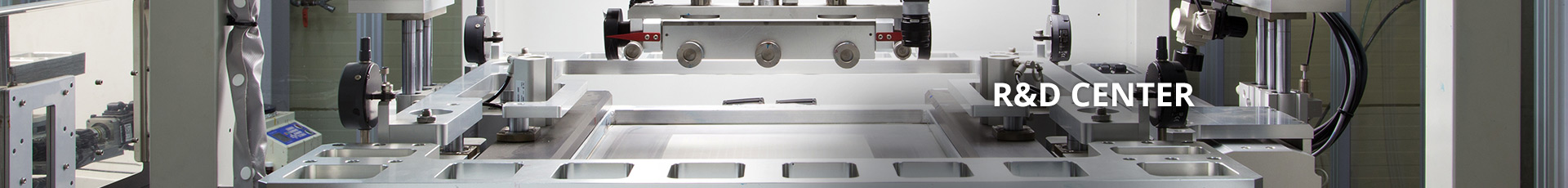
Printed Electronics Lab > R&D CENTER > R&D CENTER
성안 인쇄전자연구소(SAM Printed Electronics Lab)는 OPV, OLED, Electric Circuit 등의 다양한 인쇄전자 어플리케이션 공정 및 장비 기술개발을 위해 설립된 특화 연구소입니다. 지난 5년간 SPEL은 인쇄전자 분야의 생산장비, 제어, 인쇄, 코팅, 건조/경화 기술을 포함하는 다양한 국가 과제를 성공적으로 수행해 왔으며 이와 관련된 제조기술 개발을 선도하고 있습니다. 당사의 롤투롤 (Roll to Roll) 기반 생산공정 기술에 대한 독보적인 노하우는 고객에게 turnkey base 시스템 기술로 제공 가능하며, 유연 인쇄전자 비즈니스를 원하는 고객에게 신뢰성 있는 최첨단 생산 기술제공을 약속합니다.
SPEL for Printed Intelligence
SungAn Printed Electronics Laboratory specializes in developing Since the last decade, SPEL has been focused on developing The turn key system technology with roll to roll based 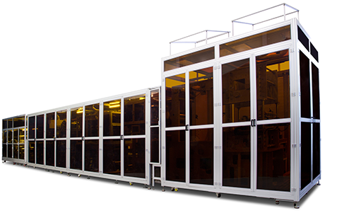
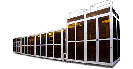
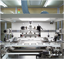
RCC Series
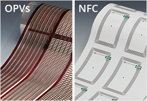
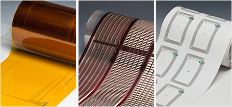
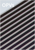
Applications
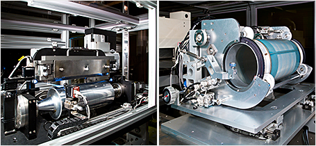
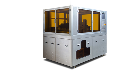
RSC-P Series
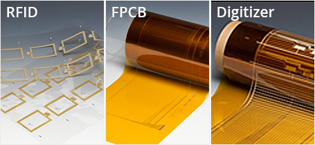
Applications
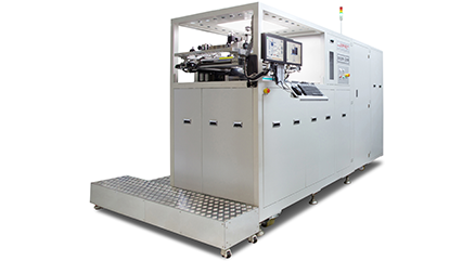
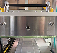
SSDC Series
Applications
Core technology of printed electronics
R2R based direct metal etching system
Advantage of direct metal etching paste Conventional wet etching process 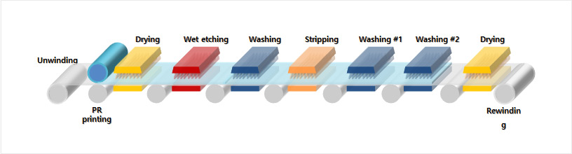
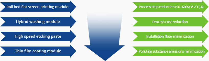
R2R hybrid etching process (with etching paste) 
Ultra high quality barrier film production system
Advantage of SAM’s ultra high barrier technology
Conventional barrier film tech 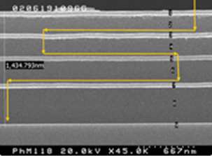
Increase moisture/ oxygen diffusion path length 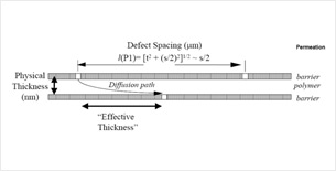
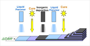

SAM’s barrier film tech 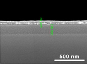
Reduce defect / pinhole of layer 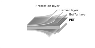

|